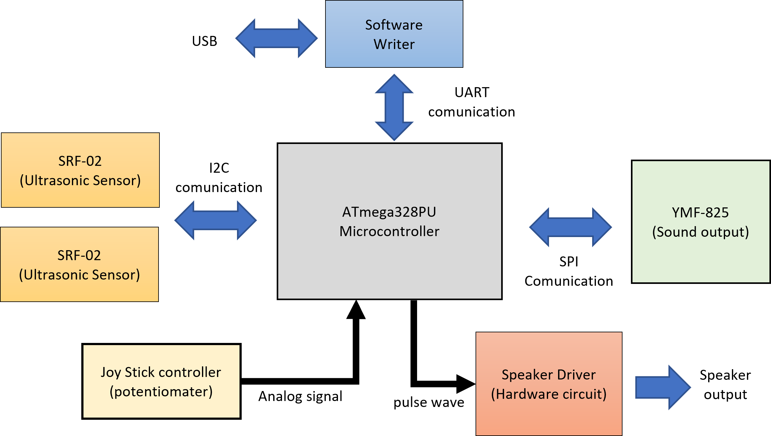
In the previous blog, I even designed a block diagram of an ultrasonic musical instrument. I will start circuit design at once. The following is the block diagram designed last time.
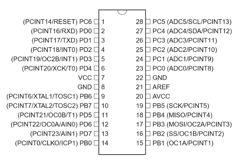
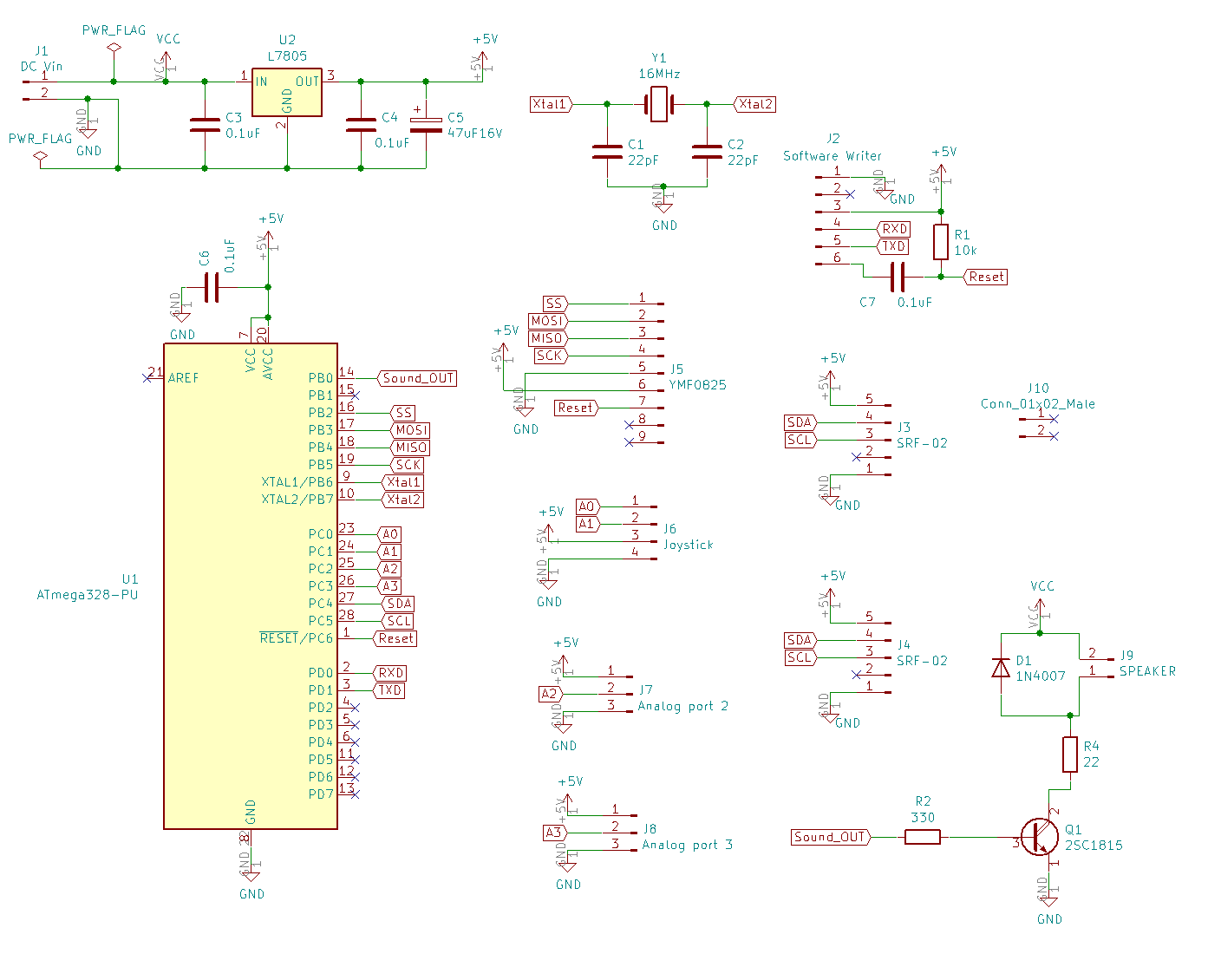
In short, how to connect each module to the microcomputer is important. First, check the pin layout of the microcomputer to be used.
pin asign ATmega328PU
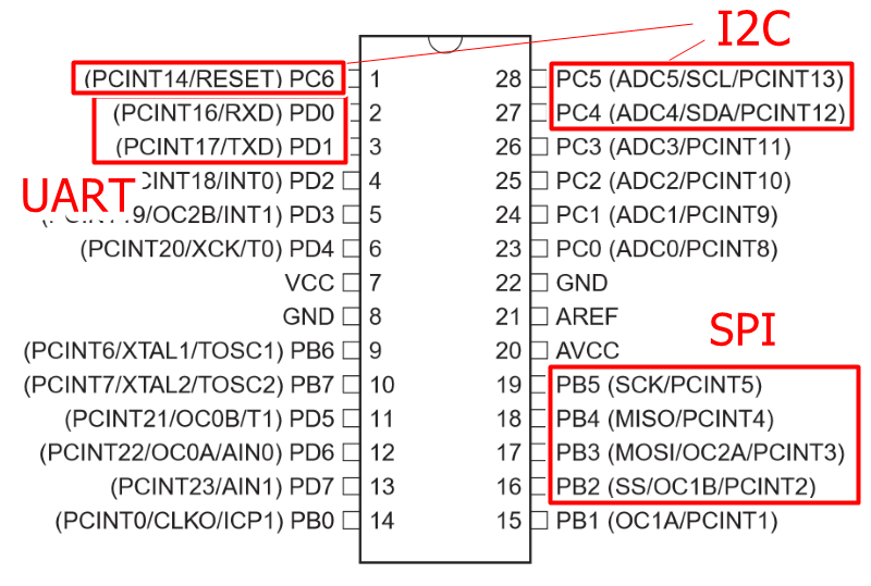
Communication port of ATmega328PU
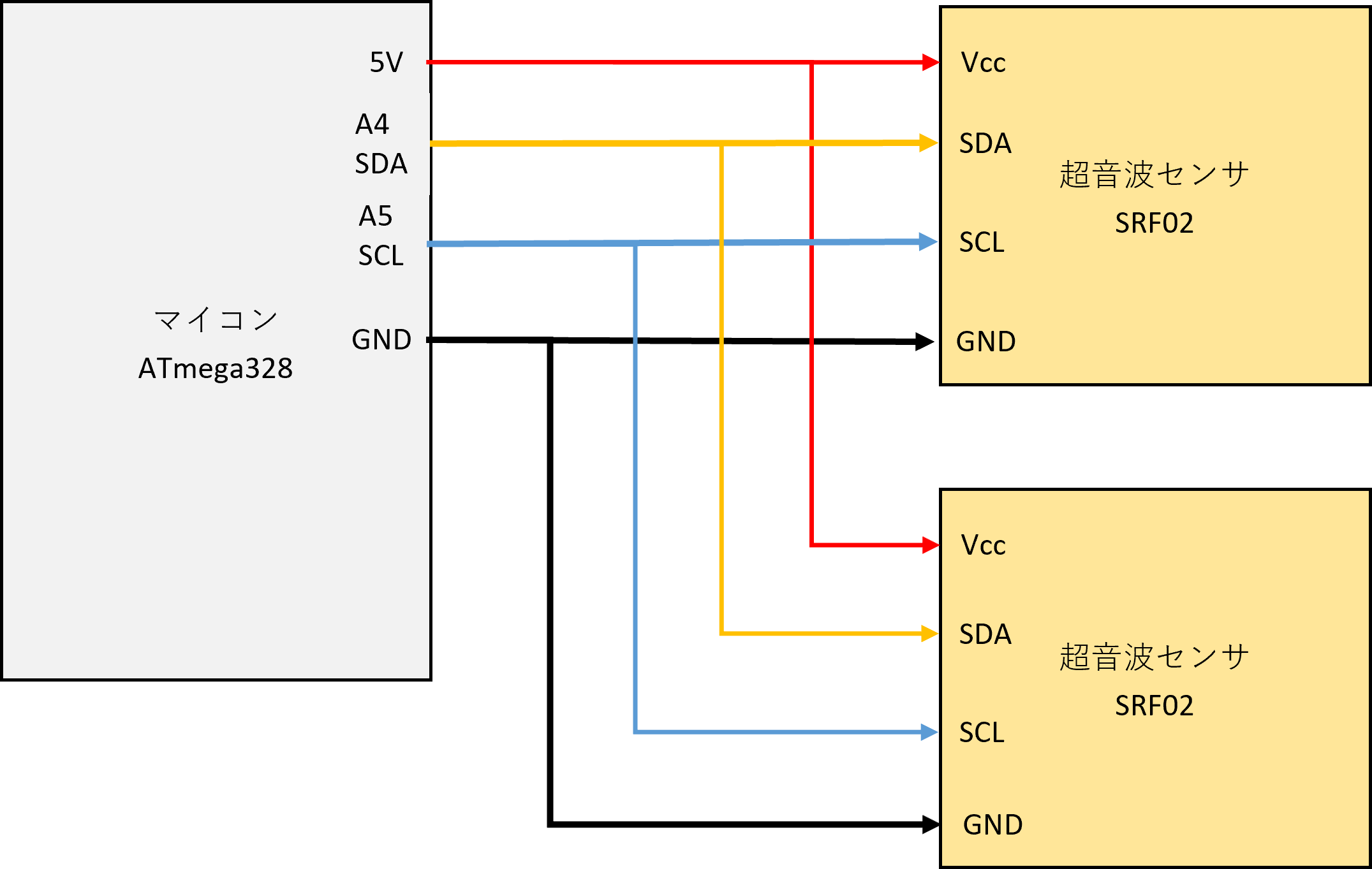
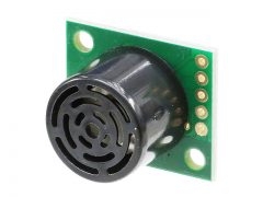
Connected to SRF-02
SRF-02 communicates in the format of I2C.
I2C connection method is very easy. This time, we will make it possible to connect two ultrasonic sensors in parallel.
For I2C communication, connect the four terminals of Vcc and GND power supply terminals, synchronous clock SCL, and signal line SDA of the sensor (Slave) and microcomputer (Master), respectively.
Even if they are connected in parallel, there is no problem because the addresses are assigned to each sensor.
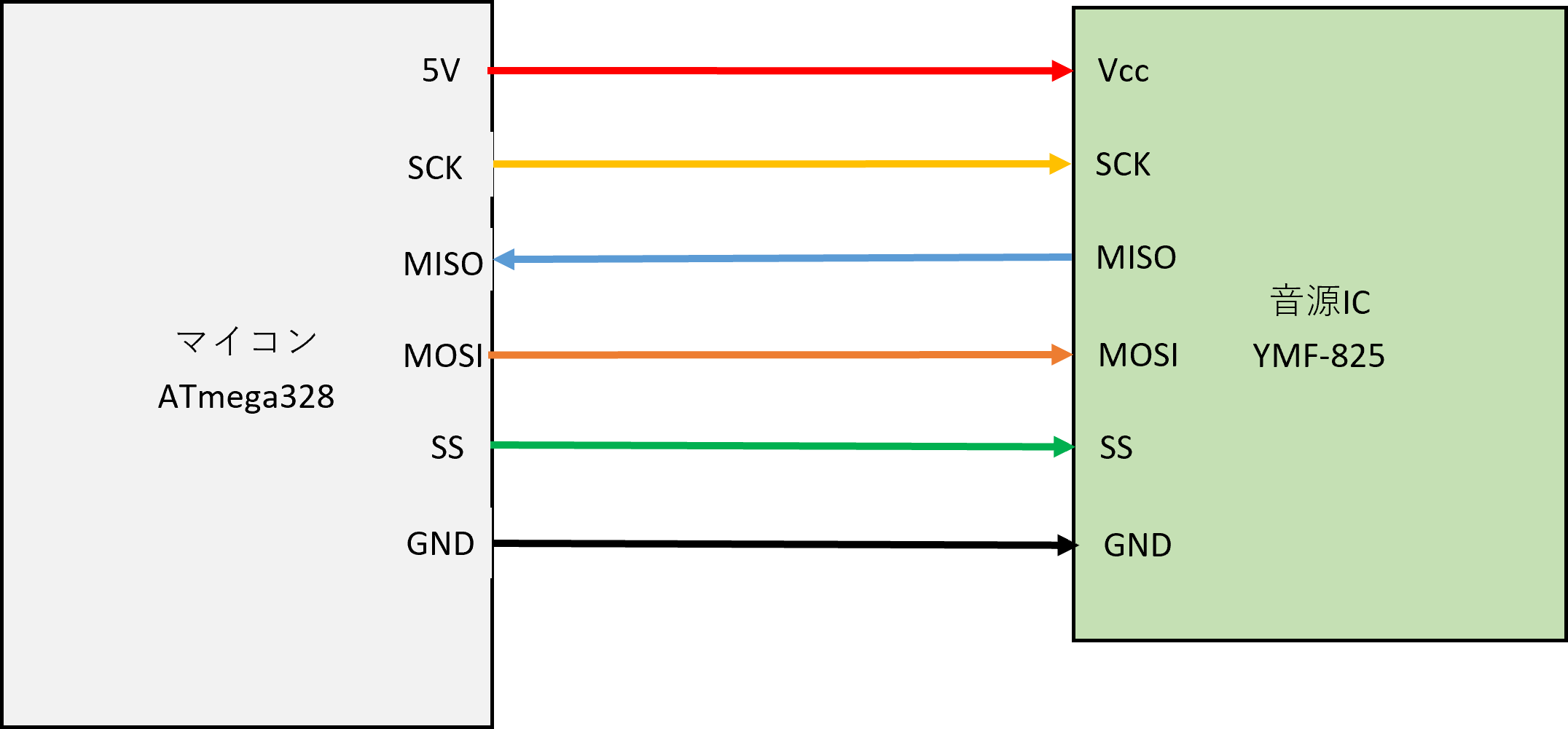
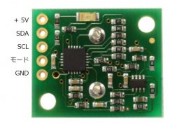
Connected to YMF-825
YMF-825 communicates by SPI.
SPI communication is from Vcc and GND power terminals on the sound source IC (Slave) and microcomputer (Master), SS (Slave Select) that selects the SCK of the synchronization clock and the Slave to be connected, and from Master to Slave. There are MOSI (Master Out Slave In) that sends a signal and MISO (Master In Slave Out) that sends a signal from Slave to Master, and it consists of a total of 6 lines.
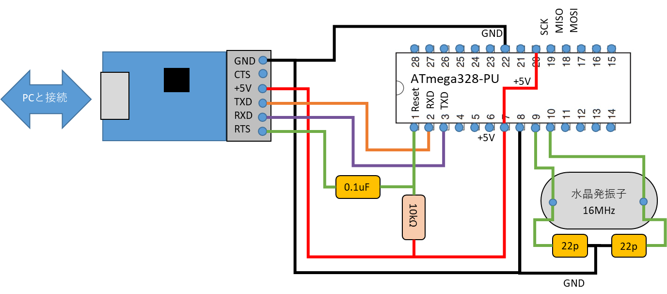
Since soft writing communicates via UART, connect the TXD (transmission) of the converter to the RXD (receive) of the ATmega328, and connect the RXD (receive) of the converter to the TXD (transmission) of the ATmega328. After that, the + 5V and GND of the TTL converter are also supplied to the ATmega328. Then, connect the RTS and the ATmega328 Reset via a 0.1uF capacitor so that the converter can send a reset signal.
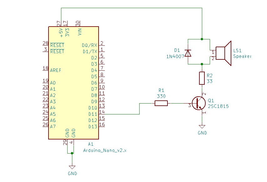
Speaker Driver
Depending on how you use YMF-825, you may run out of memory. For such a case, we have prepared a speaker driver circuit that can produce simple electronic sounds.
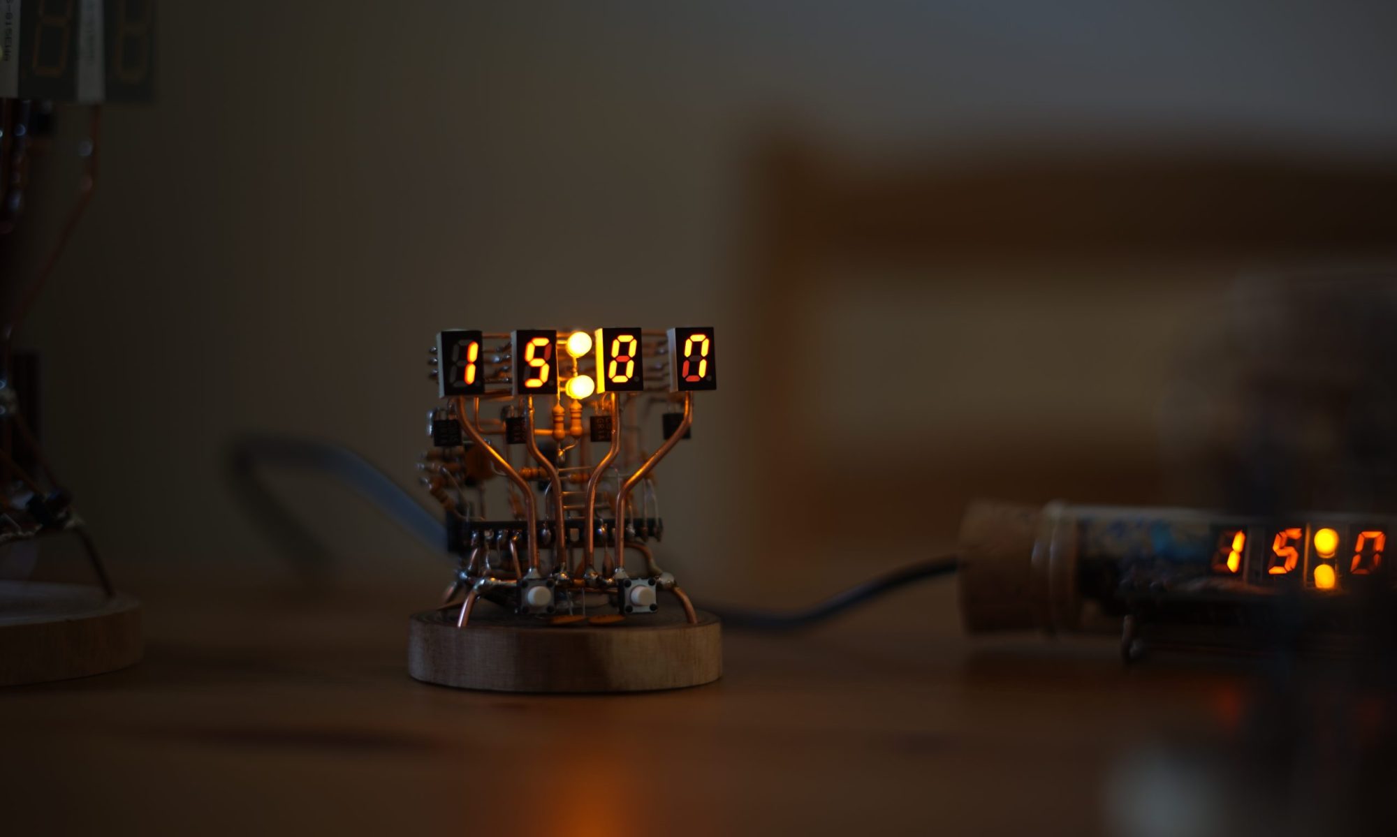
This is a new project from this time. I would like to make a new musical instrument. For this blog, I would like to do everything from the concept to the design of the block diagram.
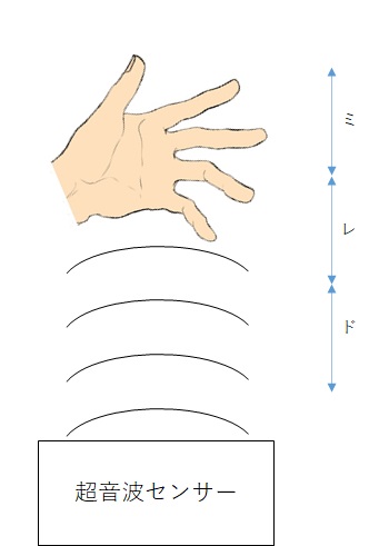
Image of new musical instrument
The image shows the ultrasonic sensor facing up as shown on the right.
Hold your hand over the sensor to play. It is a simple scale whose scale is determined by the height of the hand you hold it over.
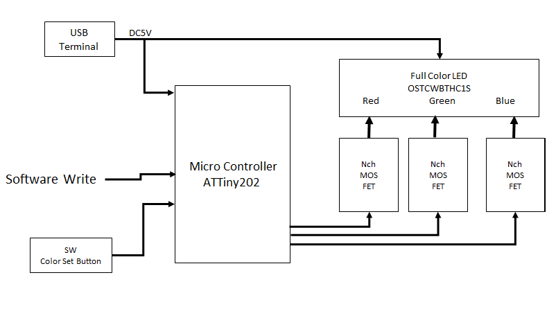
Block Diagram
Next is a block diagram.
The main microcomputer uses ATmega328 for the convenience of being easily programmed with Arduino. SRF-02 was used for the ultrasonic sensor. Allows you to connect up to two sensors. Information is transmitted between the ultrasonic sensor and the microcomputer by I2C communication. Also, connect the module YMF-825 that uses YAMAHA’s sound source IC that can create various tones. This exchanges information via SPI communication. After that, a joystick that allows you to manually enter the timing of making sounds. And, in case the YMF-825 and the ultrasonic sensor cannot be operated at the same time due to the memory over of the microcomputer, etc. It also has a circuit that can drive the speaker directly. Also, since the microcomputer operates independently, it is necessary to prepare a software write terminal. Since it is still in the development stage, it will be possible to connect to the USB of the personal computer by UART communication so that the RAM value can be read.
Next, let’s take a closer look at each block.
Microcomputer
The microcomputers to be used are summarized below on the Akizuki Denshi sales page.
ATmega328 (秋月電子HPより引用) ATmega328 (秋月電子HPより引用)
It is a memory doubled version of ATmega168. The one in which a program called a boot loader is written is one of the popular microcomputers in electronic work such as being installed in Arduino.
Sound is produced by directly controlling the YMF825 register from a microcomputer board such as Arduino or Raspberry Pi through SPI. Since it also has a speaker amplifier, there is no need to prepare an amplifier circuit separately.
* Although it is equipped with a 3.5 mm headphone jack, earphones that use 4-pole CTIA such as for iPhone cannot be used (OMTP ones can be used). ** From Switch science’s sales page **
**from Switch science**
Specifications
4 operator FM sound source
Up to 16 sounds can be produced at the same time
29 types of FM basic waveforms built-in, 8 types of algorithms
SPI Serial interface by
Built-in speaker amplifier
Built-in 3-band equalizer
Built-in 16-bit monaural D / A converter
Operating voltage: 5 V
3.3 V can also be used by modifying it
Speker Driver Circuit
About the speaker drive circuit Previous blog for a summary. Since this circuit is specialized for producing electronic sounds, I think that it is not suitable for playing ordinary music with this circuit.
The circuit is very simple. A digital output square wave is output from Arduino. This digital signal is input to the base of transistor Q1. When a current is passed through the base, the collector-emitter is turned on and the current flows through the speaker. Depending on the HIGH / LOW cycle of the digital signal, whether or not current is passed through the speaker changes. Therefore, an electronic sound having a frequency of a digital signal is emitted from the speaker.
As for the resistor of R1, the current of the digital signal is too high for the base, so the current is reduced by sandwiching the resistor R1.
Also, since the DC current flowing through the speaker is too large for the R2 resistor, the current is reduced by sandwiching the R2 resistor.
Also, with the D1 diode, if the speaker coil is turned on and off with a square wave, the speaker voltage will jump up at once, so the voltage will not jump up and the current accumulated in the speaker coil will be transferred. It is loaded with a regenerative diode to escape.
Software Writing
Regarding soft writing, I also refer to the previous blog.
Since it is UART communication, connect the TXD (transmission) of the converter to the RXD (receive) of the ATmega328, and connect the RXD (receive) of the converter to the TXD (transmission) of the ATmega328. After that, the + 5V and GND of the TTL converter are also supplied to the ATmega328.
Then, connect the Reset of RTS and ATmega328 via a 0.1uF capacitor so that the converter can send a reset signal.
After that, connect a 16MHz crystal oscillator as the clock of ATmega328.
That’s all for today. Next time, I will start circuit design.
This article is a continuation of the previous one.
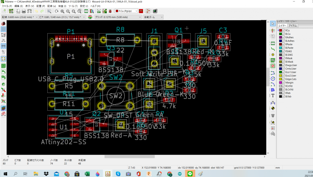
Let’s get started to designing a PCB on the KiCad software.
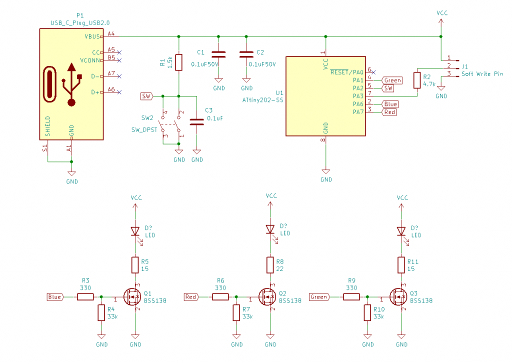
The designed circuit diagram is shown below.
Iluminate Tube PCB circuit
Associate the footprint with reference from the schematic data.
associate the footprint
Next, I will draw the wiring of the board. Need to know the size of the PCB.
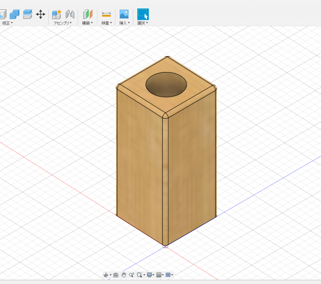
Therefore, we designed the case first that wrote by 3D-CAD.
TOP
BOTTOM
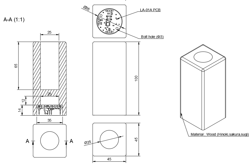
You can secure wood by buying wood with a thickness of 45 mm x 45 mm at a home center and cutting it out at 100 mm intervals.
Using a 35mm hole saw, make a hole for mounting the board from the back. Make a hole to insert the test tube with a 25 mm hole saw from the top.
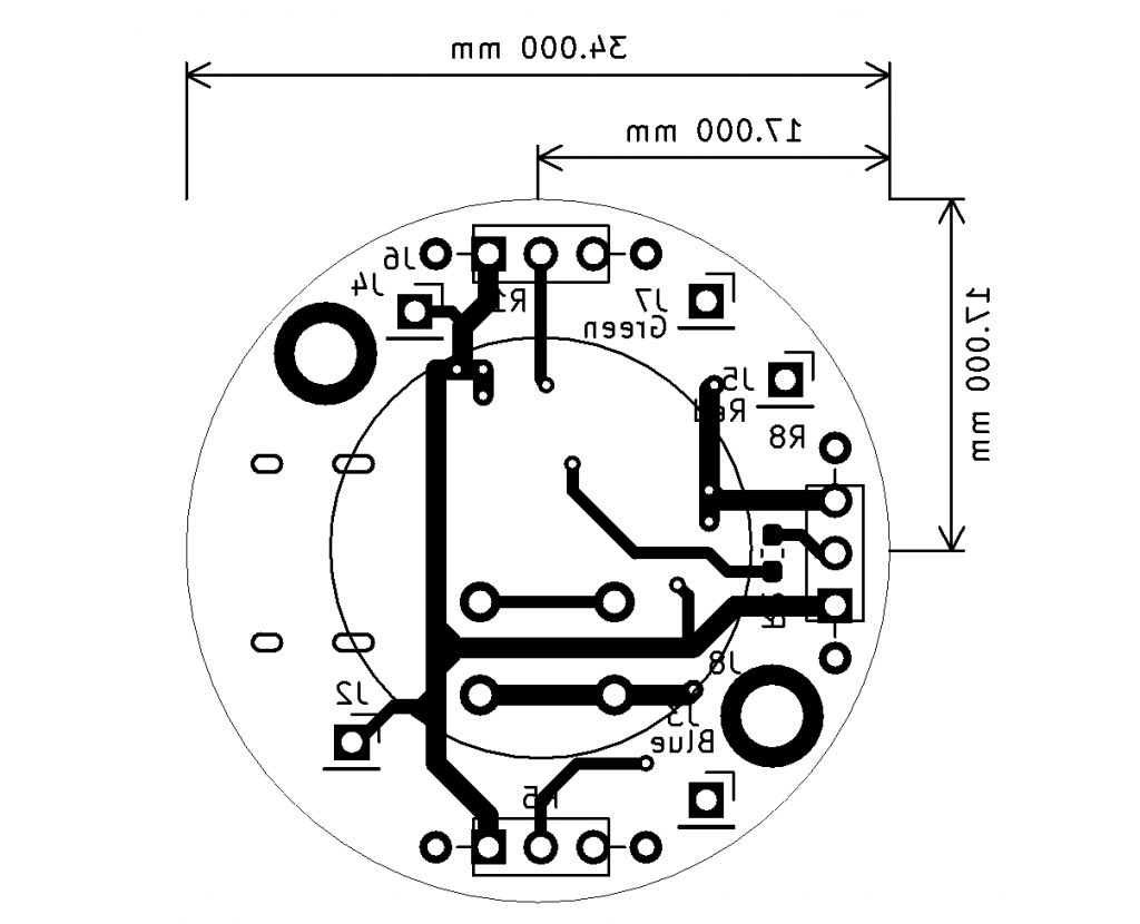
The 2D drawing is shown below.
LA-01図面
Therefore, I decided that the size to put the board in is 35mm in diameter, so I think that the size of the board should be 34mm in diameter.
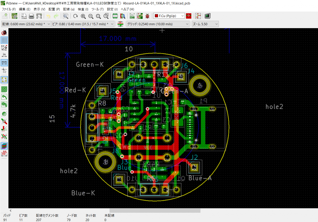
Let’s get started to design the PCB.
Board is 2 Layer.
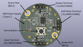
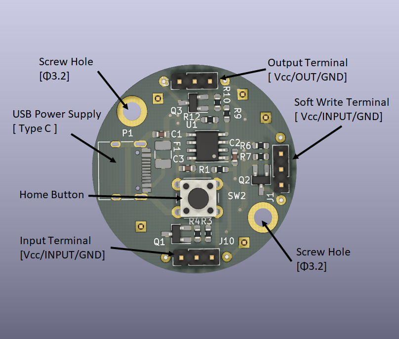
The contents of the board are shown in the figure below. Power is supplied from USB-type C.
In addition, power supply, color switching, brightness adjustment, etc. are all integrated into one home button.
After that, I would like to link the terminals for writing software and the same boards when expanding within the same product in the future. For that purpose, we have prepared a signal input terminal and an output terminal. After that, there are two screw holes Φ3.2 for fixing the board.
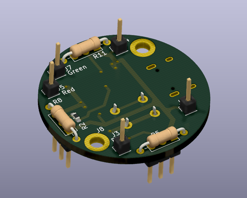
Detail of PCB
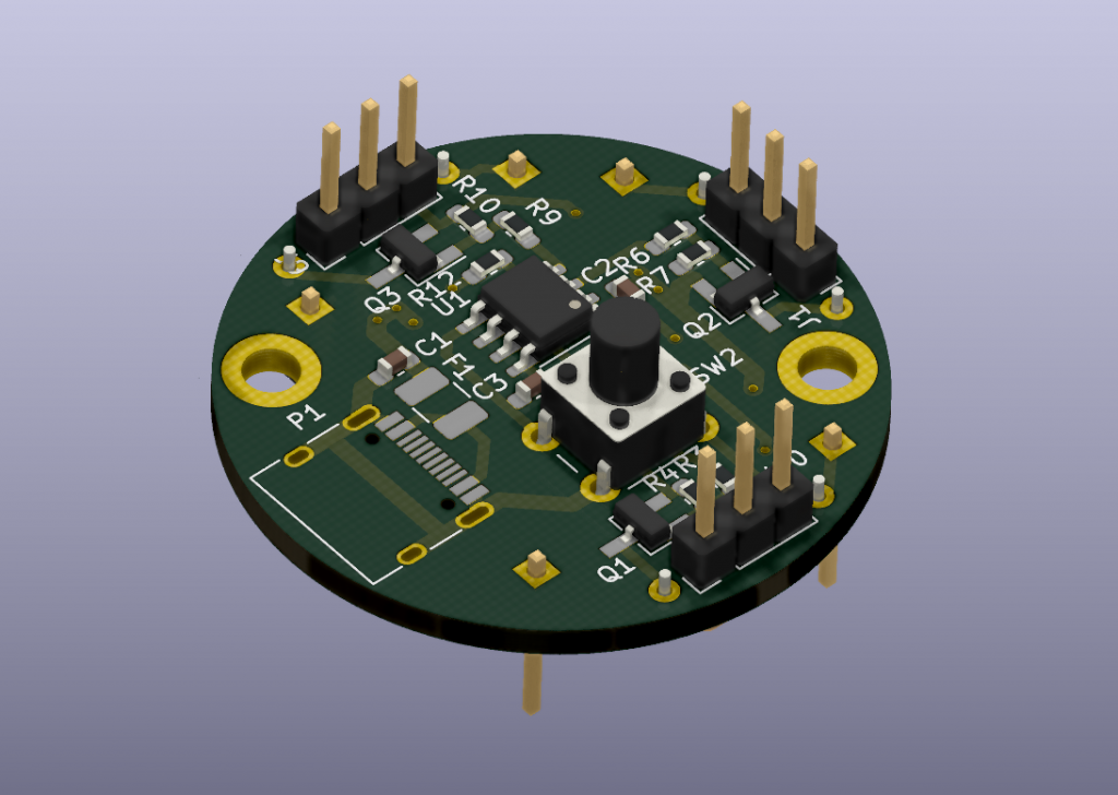
The front and back sides are shown in the figure below. There is a space in the middle of the TOP where you can place the full color LED.
PCB(Bottom)
Board(TOP)
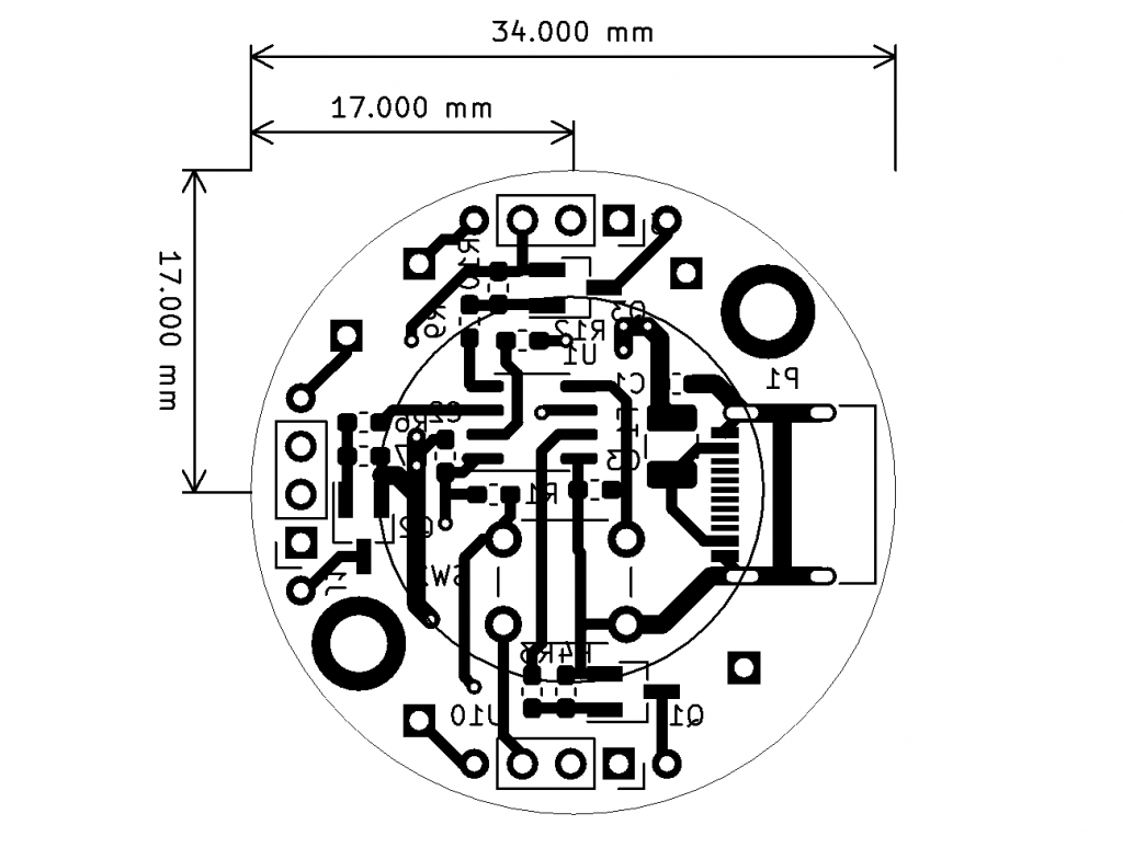
The 2D drawing is shown below.
TOP of PCB
Bottom of PCB
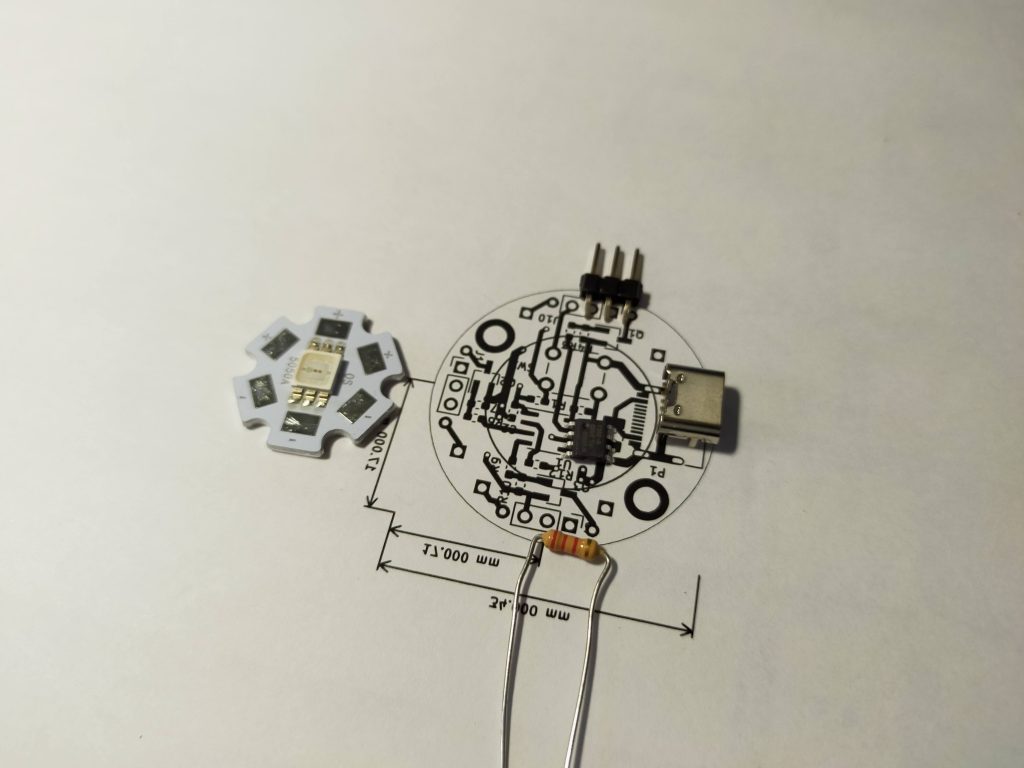
After making the drawing, we will check the actual product.
Print the drawing to full size and actually place the part on top to see if it is the correct size. This completes the design. Next time, I will order the board from a vendor.
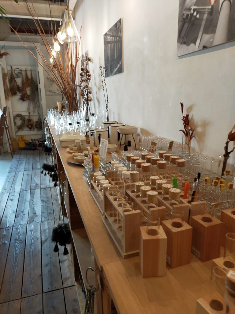
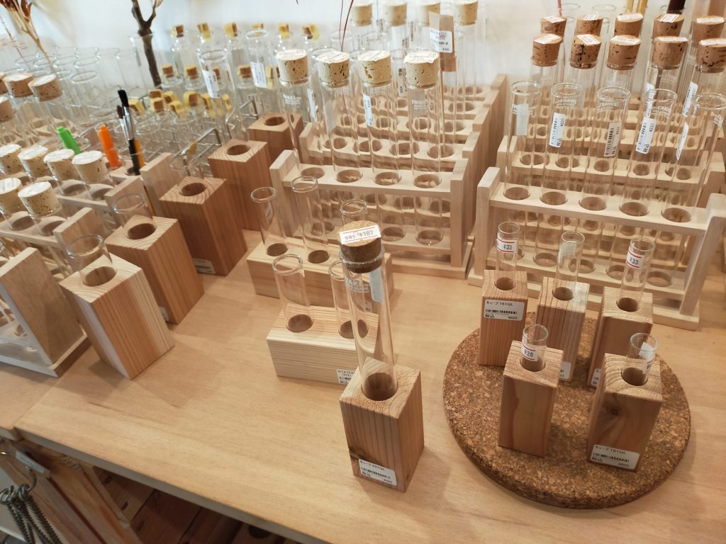
Last week. I went to the “Rikashitsu” at the Kiyosumi-Shirakawa in Tokyo. I often purchase a Cork-Glass-Tube from This shop.
The Rikashitsu is directry management shop from Sekiya Rika Co,Ltd a wholesaler of glass for science and medicine. This shop is aims at “physical chemistry + interior”.
This sells science and chemistry products actually used by professionals and Original product processed by Glass Craftmen.
The reason why this shop was opened that the craftsman’s skill could be utilized by getting ideas by using physics and chemistry glass products by the general public.
There was a very stylish space inside the shop. I felt that the science experiment was very photogenic.
I am amaized from new value.
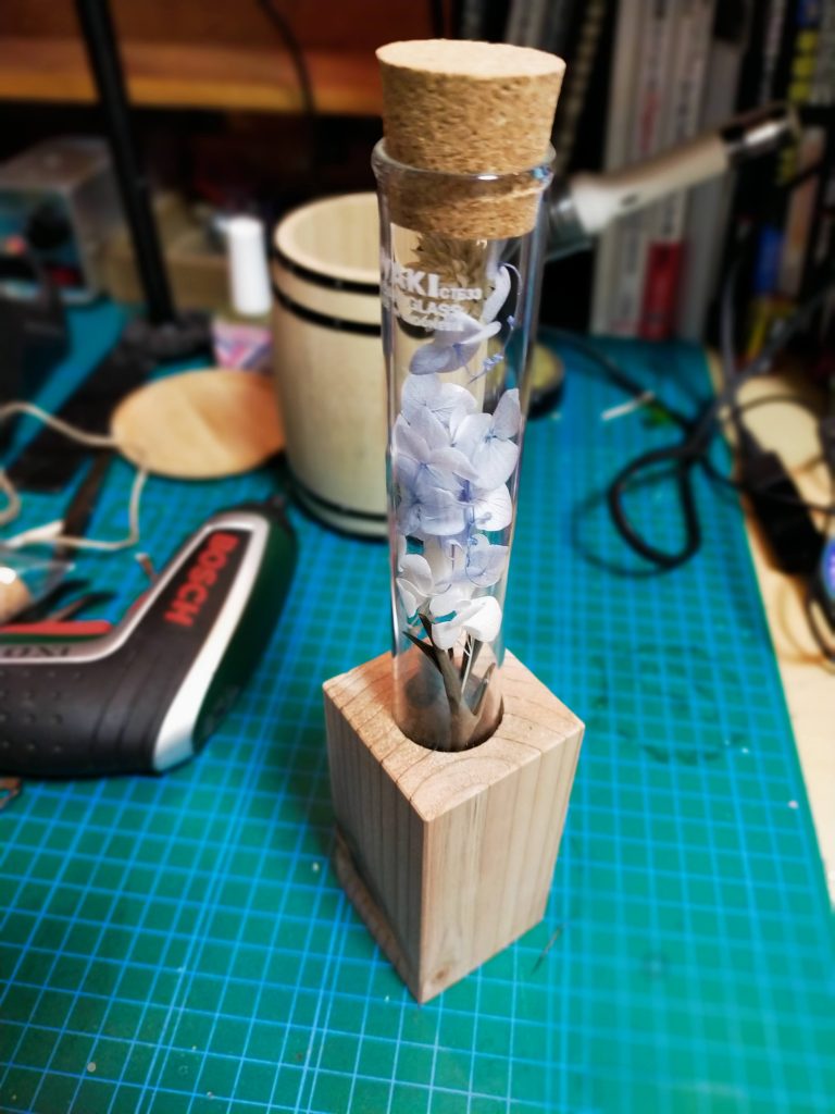
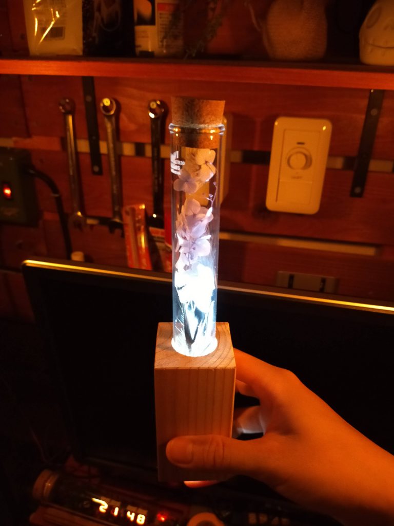
I impulsiverly bought a Cork Glass Tube and Woodern Stand at this shop.
Cork Glass Tube
Woodern Stand
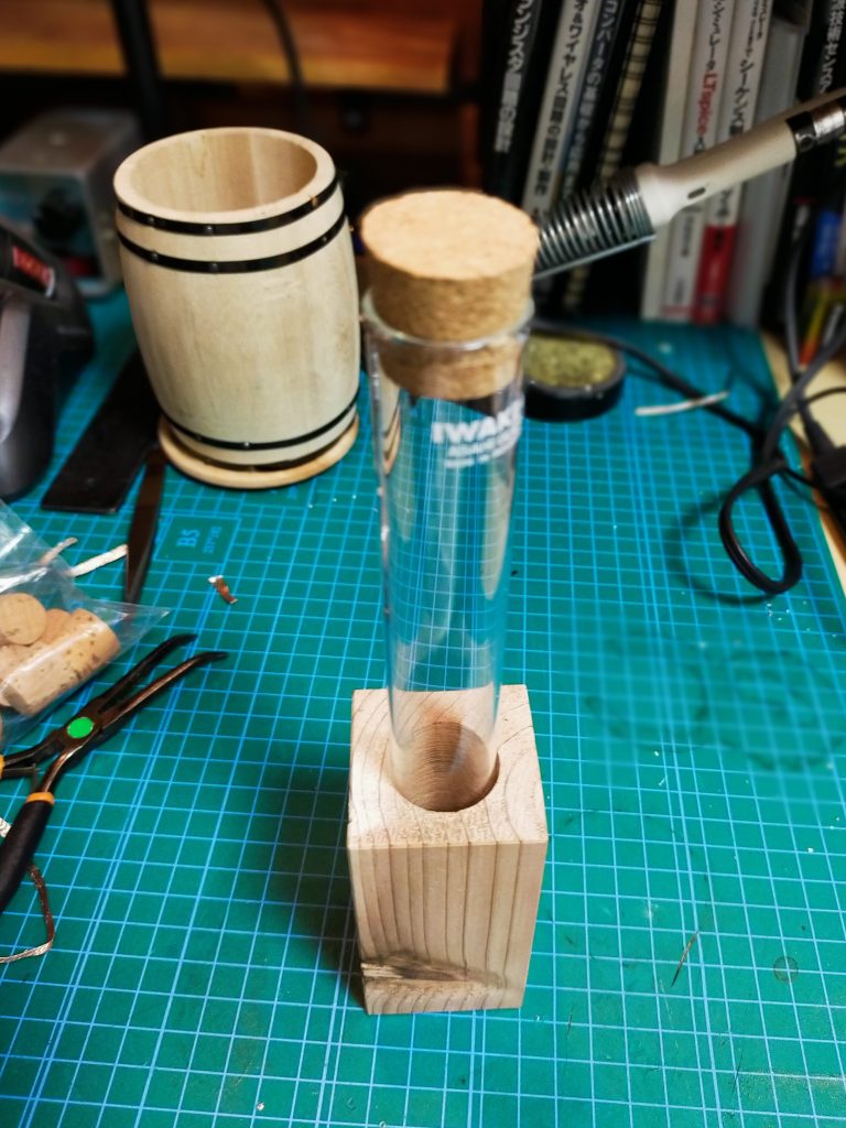
From the moment I saw it at the store, I strongly wanted to make it Iluminate.
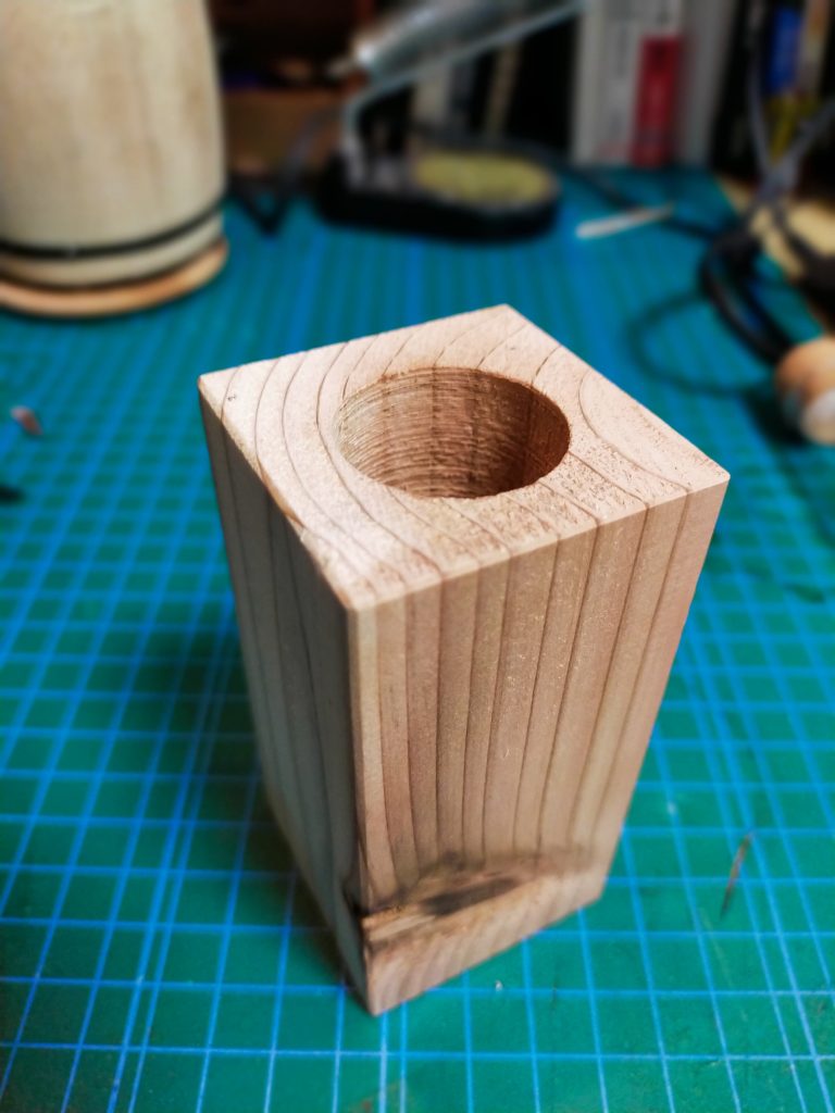
As soon as I got home, I remodeled a Woodern Stand.
I made a hole in the back of the stand with a drill and packed artificial flowers in the Glass Tube.
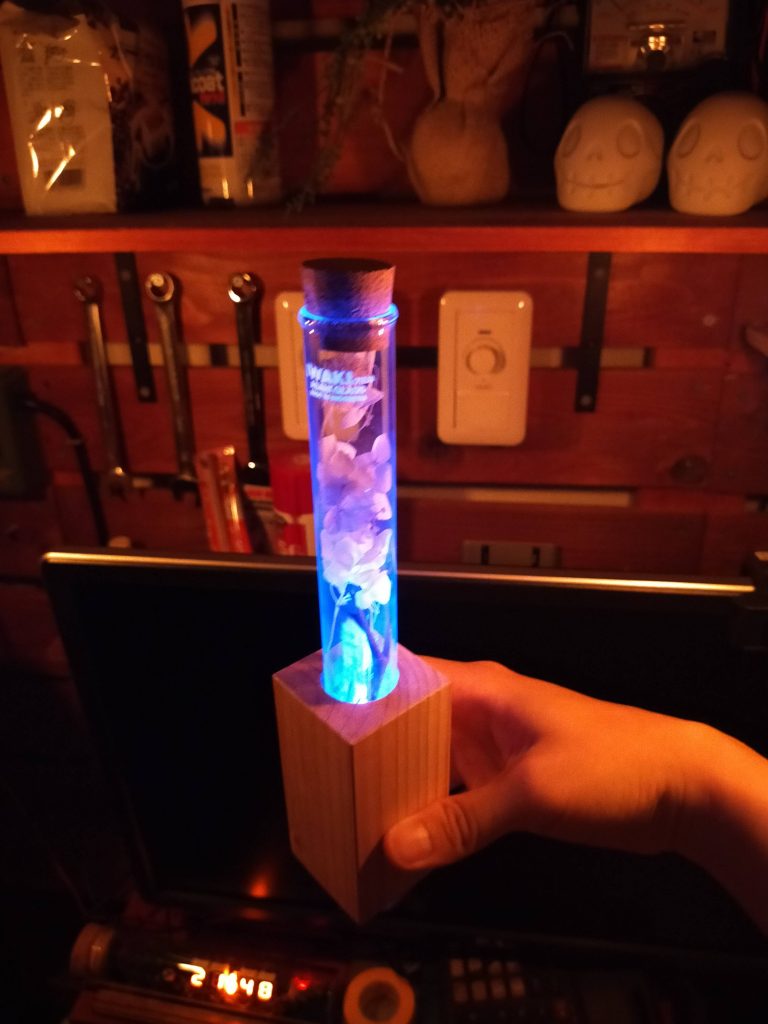
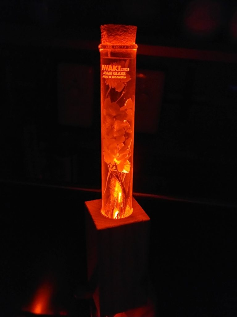
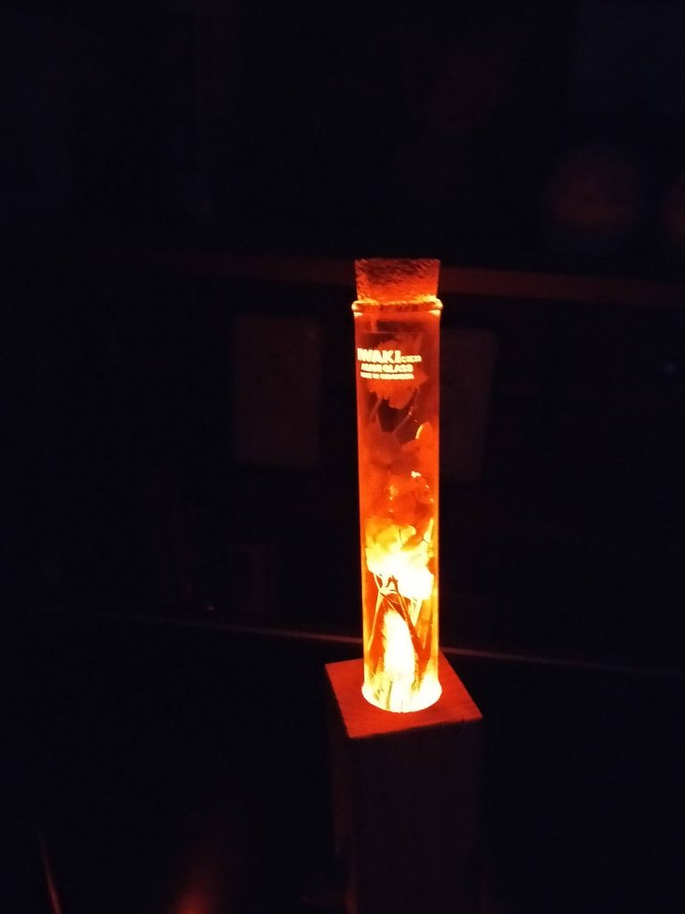
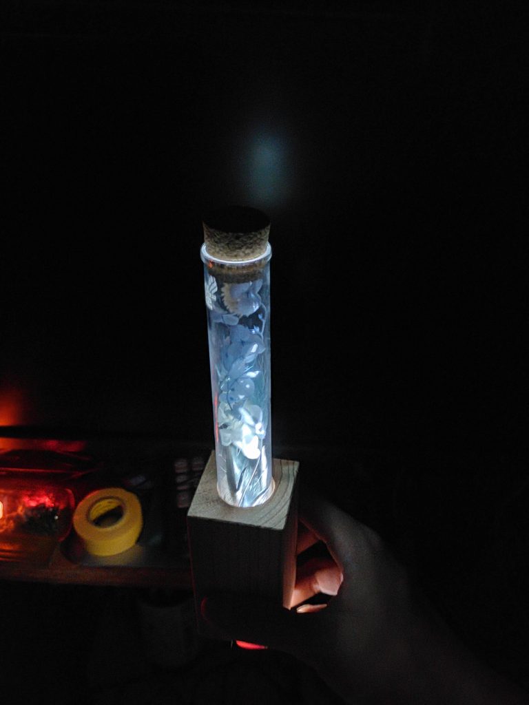
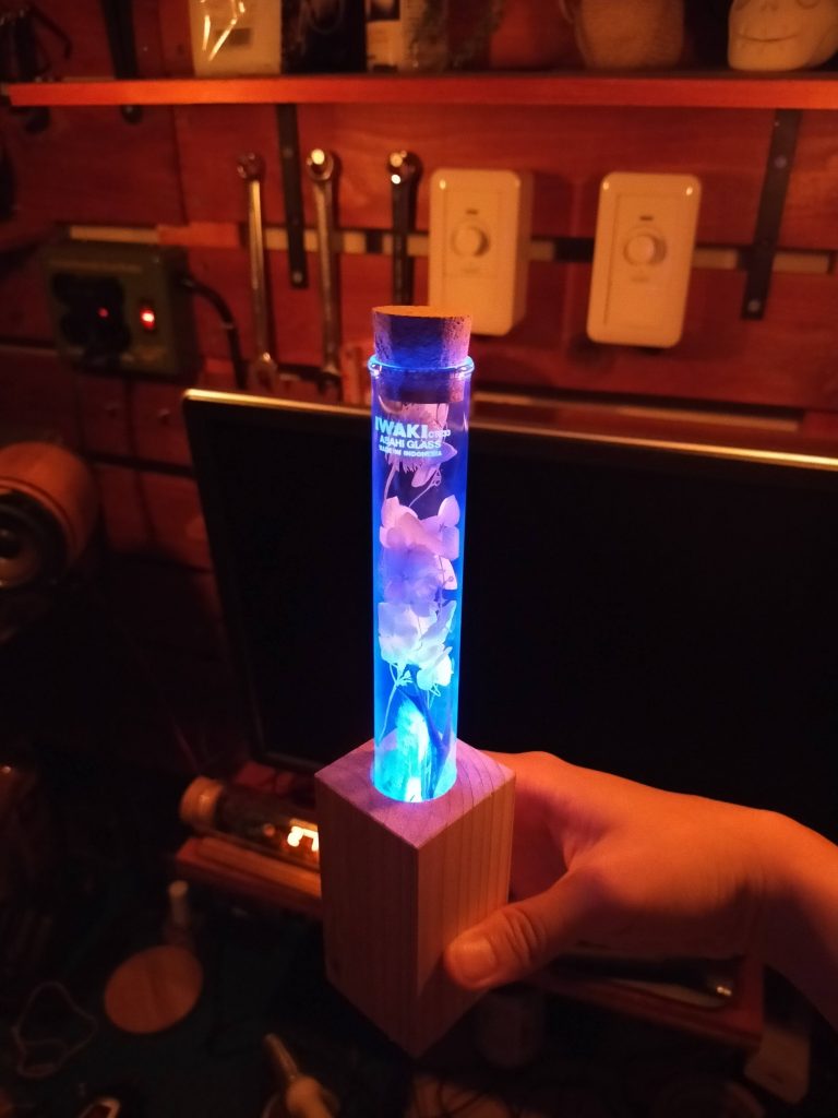
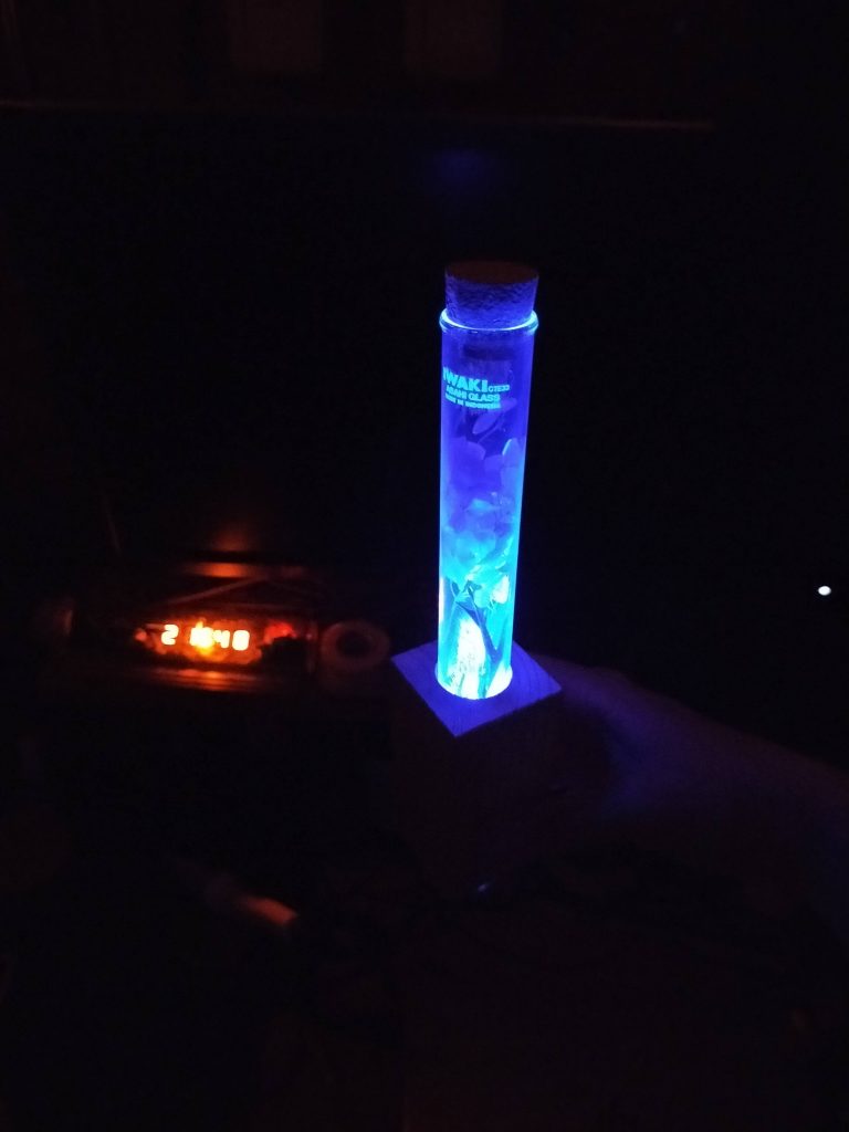
The photo below shows the actually Glass Tube illuminated.
I inserted an LED through the hole to make the Glass Tube Iluminated. This is very Good.
This will quickly make the Print Circuit Board.
I would like to make it possible to Iluminate in any color using a Tiny-Microcomputer and a full-color LED.
size of microcomputer(from Akitsuki-Denshi Home Pages)
The memory capacity of this microcomputer is only 2kB.
Is it about 2000 half-width text characters? Since the capacity is very small, only simple programs can be written.
However, this should be enough if it only illuminates a three-color LED.
Next, the LED specifications are shown below.
For the LED, I adopted a full-color LED containing the three primary colors.
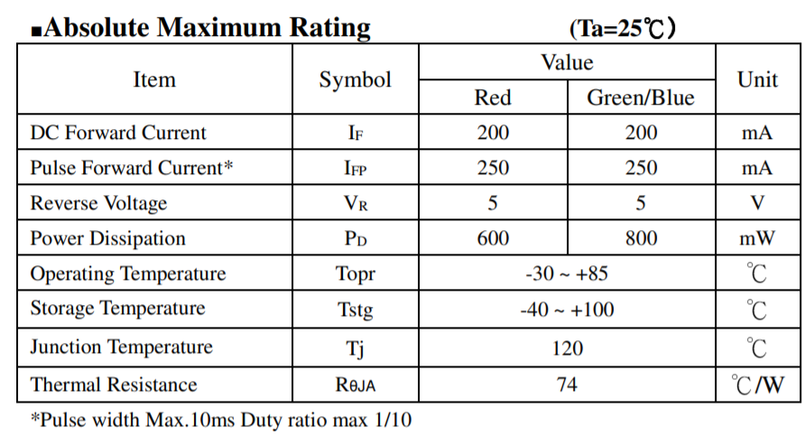
DC Forward Current:150mA Power Dissipation: 1W
・VF: Red…2.5V Blue、Green 3.3V
・ΦV:
Red…22lumen
Green…35 lumen
Blue…12 lumen
・λD: Red…624nm Green…525nm Blue …460nm ・2θ1/2:120°
size of LED chip(from Akitsuki-Denshi Home Pages)
Power Dissipation is 1W. The standard current is as high as 150mA. It’s very dazzling.
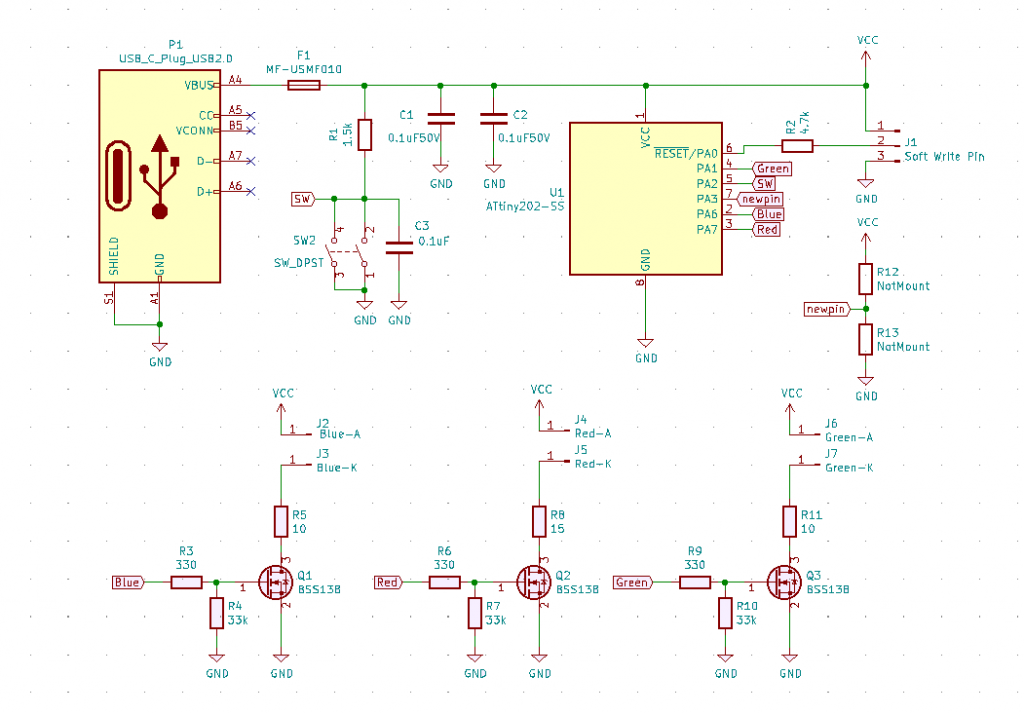
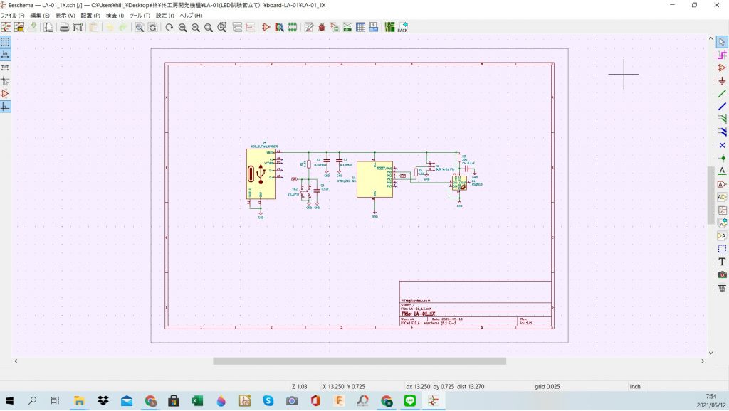
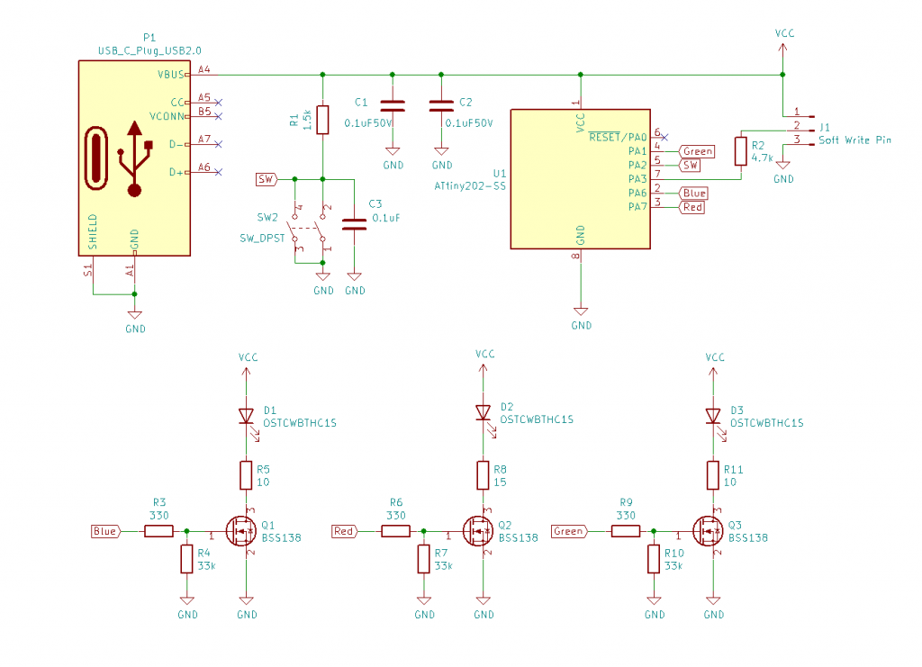
I wrote the electric circuit diagram below.
LA-01 回路図
The Full color LED used has a very high current. it is difficult to operate it by connecting it directly to the output terminal of the microcomputer.
Therefore, Increase the current by connecting an N-channel MOSFET to each LED.
The brightness of the LED is adjusted by the PWM signal from the microcomputer.
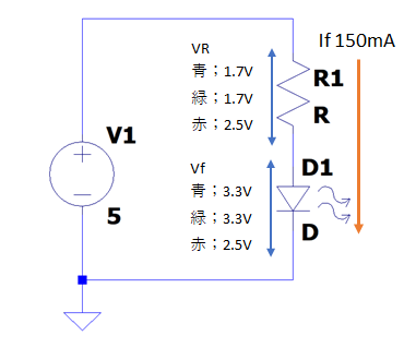
Wrote the calculation of limiting resistance(R5,R8,R11) connected to LED below.
IF the MOSFET is turn ON completely that can be only resistor and LED on the circuit by omitted MOSFET.
The information required for the calculation is the standard current and voltage of the LEDs below.
IF=150mA VF:Red…2.5V Blue Green 3.3V
The value obtained by subtracting the LED Vf from the power supply voltage is the voltage between the terminals of the resistor.
Since a current of 150mA is passed through the resistor and LED, the calculation result of the resistance value of the limiting resistor is as follows.、
Blue; R=V/I = 1.7V / 150mA = 11.33[Ω]
Green; R=V/I = 1.7V / 150mA = 11.33[Ω]
Red; R=V/I = 2.5V / 150mA = 16.66[Ω]
However, the right resistance value is not sold on the market. The resistors sold on the market follow the E24 series, with the closest values is below.
blue; 11.33[Ω]=10Ω
Green; 11.33[Ω] =10Ω
Red; 16.66[Ω] =15Ω
next, Calculate the actual current when this resistance value is applied.
Blue; Current If [mA] = V/R = 1.7 / 10 =170 [mA]
Green; Current If [mA] = V/R = 1.7 / 10 =170 [mA]
Red; Current If [mA] = V/R = 2.5 / 15 = 166[mA]
Make sure that the calculated current value is less than the rated current value listed in the LED data sheet.
Absolute Maximum Rating on the LED datasheet
Since the DC rating of the LED is 200mA, there is a surplus of about 30mA.In addition, since this unit performs PWM control, the value of “Pluse Forward Current” in the data sheet is applied. Then, the rating becomes 250mA, and there is sufficient margin even if the error of resistance is taken into consideration.
The voltage between the resistor terminals should be low due from the power loss of the FET.
Next, Calculate to the Power Loss of the Resistors below.
Blue; Power Loss of the Resistor(Blue) Pr [W] = V * If = 1.7 V*170mA = 289 [mW]
Green; Power Loss of the Resistor(Green) Pr [W] = V * If = 1.7 V*170mA = 289 [mW]
Red; Power Loss of the Resistor(Red) Pr [W] = V * If = 2.5 V*166mA = 415 [mW]
Only the red color is prominent and the loss is large.
For the above reasons, use a resistor with a rating of 0.5W or more.
Next is the selection of FET.
Since a maximum current of 170mA is flowing between the drain and source of the FET, it is necessary to allow more drain current to flow. I chose BSS138 because of its price and performance.
BSS138 (from Akitsuki Denshi Home pages)
・Construction:MOSFET ・Number of circuits:1 ・channel:N ・Voltage between drain and souce:50V ・ Voltage between gate and souce :±20V ・Current of Drain(DC):300mA ・ON resistance between drain souce:1.6Ω ・Tolerance of Power Loss(25℃):350mW ・Package:SOT-23
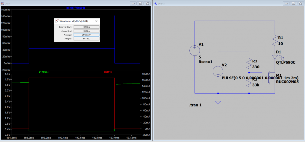
Next Calculate the Power loss of FET.
We simulated FET loss with LTSpice. I wish I could use the BSS138 Spice model, but I couldn’t add it successfully. Therefore, we simulated with a FET model with similar values of Rds and Vds.
シミュレーション結果
The Joule integral value of the power obtained by multiplying Ids and Vds from this value was 44.49uJ.
Since the PWM pulse is 500Hz, 500 * 44.49u = 22.24 mW
The thermal resistance θjc of this FET is 350 ° C / W.
When the temperature is 25 ° C, the junction temperature is Tj = 25+ (350 × 0.02224) = 32.78 ° C.
Even with the maximum current, the temperature rises by + 7.78 ° C, so I don’t think it will have much effect.
Ciruit
For the above reasons, it is decided by this circuit diagram. Next, design the board based on this. see you next time.