We will design the circuit of the circuit block designed in the block diagram last time.
The block diagram shown last time is shown below.
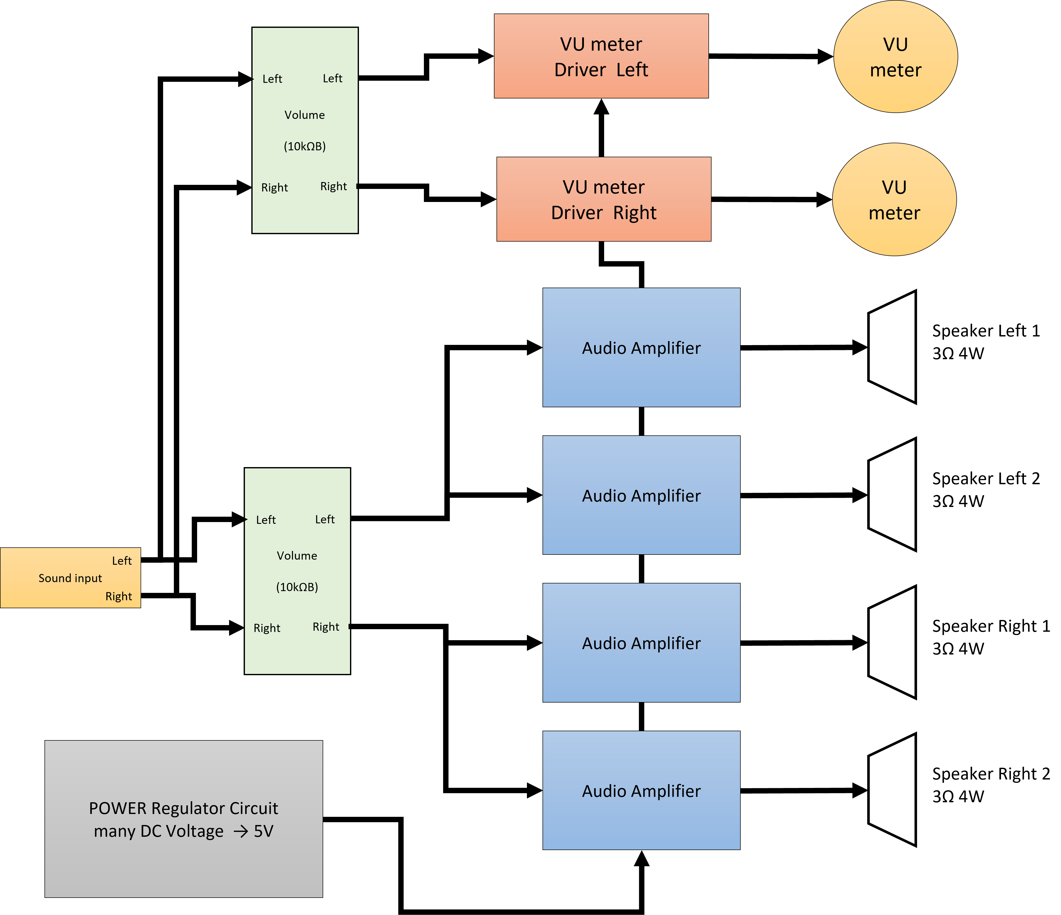
There are three circuit blocks that have design elements here. Audio Amplifier, Power Regulator, and VU meter driver.
First, the circuit diagram of the designed amplifier is shown below.
Audio Amplifer
This is an amplifier Circuit below.
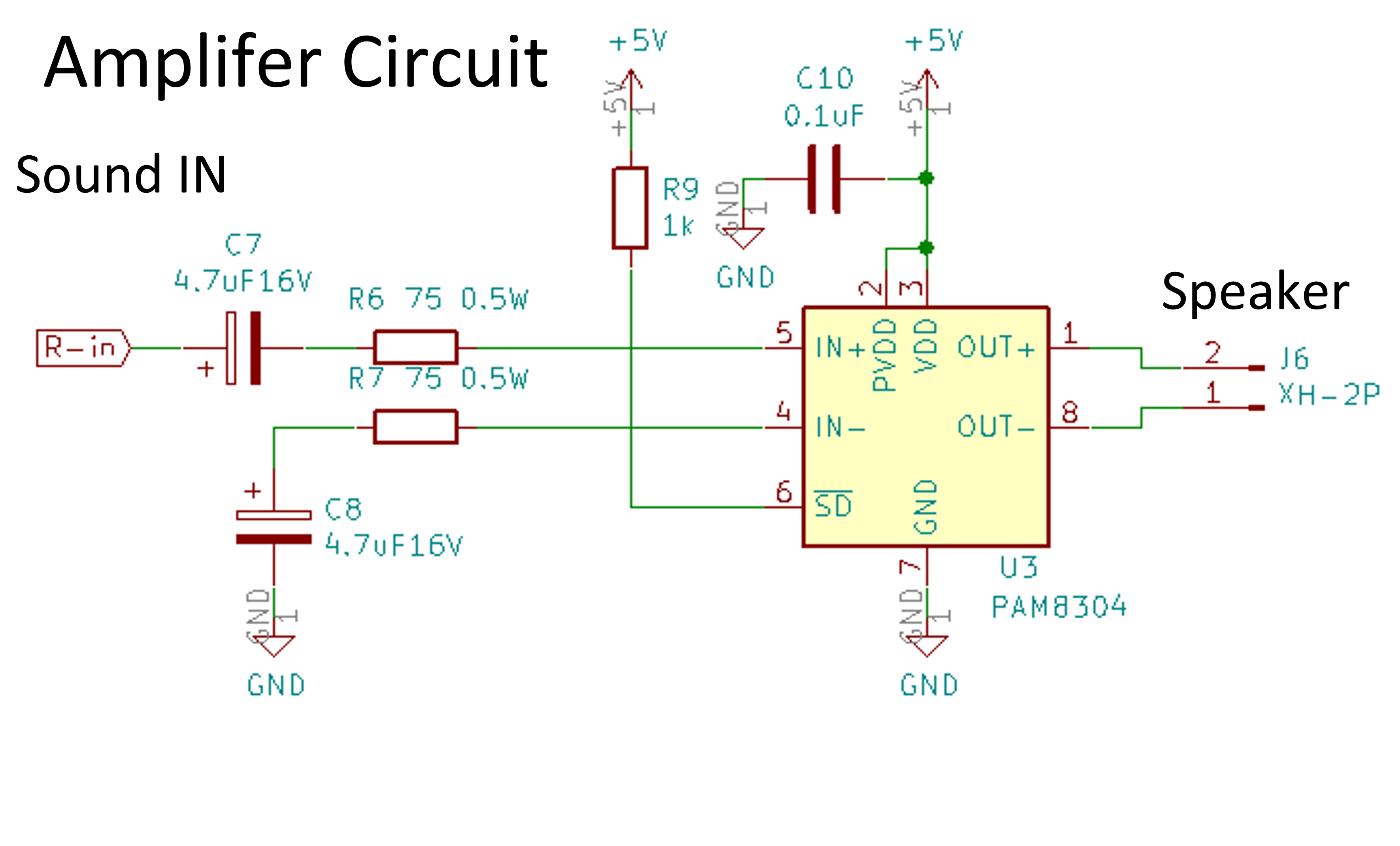
I used an amplifier IC (PAM8304) that does not require detailed design.

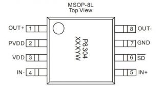
D Class Amplifer IC PAM8304ASR
■Summary
・Power Voltage:2.8~6V
・Output:
3W typ(5V・4Ω)
1.75W typ(5V・8Ω)
・Gain:300000/Rin
(30倍 about Rin 10kΩ)
・Loss Current at No signal:5mA typ(VDD=5V)
・Power efficiency:93% typ(RL=8Ω、THD=10%)
・Package:0.65mm、MSOP8
**Quoted from HP of Akitsuki denshi**
For the circuit, I used the reference circuit described in the data sheet here. The resistance value and the capacitor were decided sensuously.
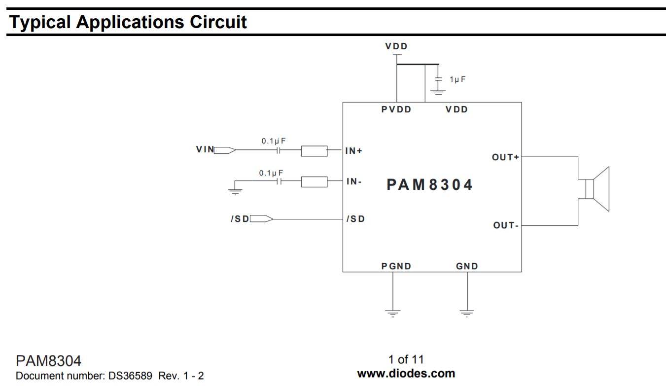
The SD (shutdown) terminal is pulled up because it will stop unless it is pulled up.
VU meter circuit
Next is the circuit of the VU meter.
The VU meter is, so to speak, a DC ammeter. Instead of inputting the audio signal directly, it is amplified by an operational amplifier, rectified by a diode (converted from AC to DC), and the current is adjusted by a resistor and sent to the VU meter.
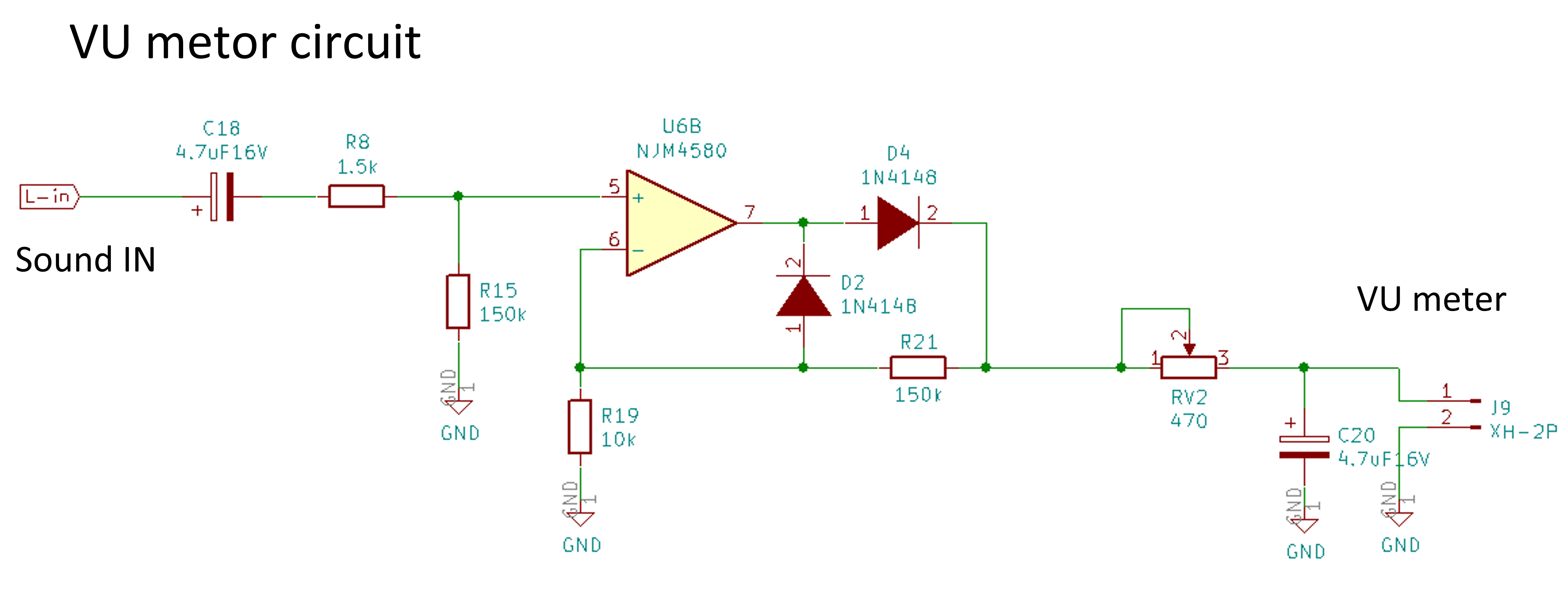
For the OPAMP, I used NJM4580, which can be used for general purposes.
Power Regulator Circuit
Next is the power supply circuit.
Since the power supply voltage of the amplifier ICPAM8304 is 6V at maximum, a circuit that can flow a constant voltage of 5V is required.
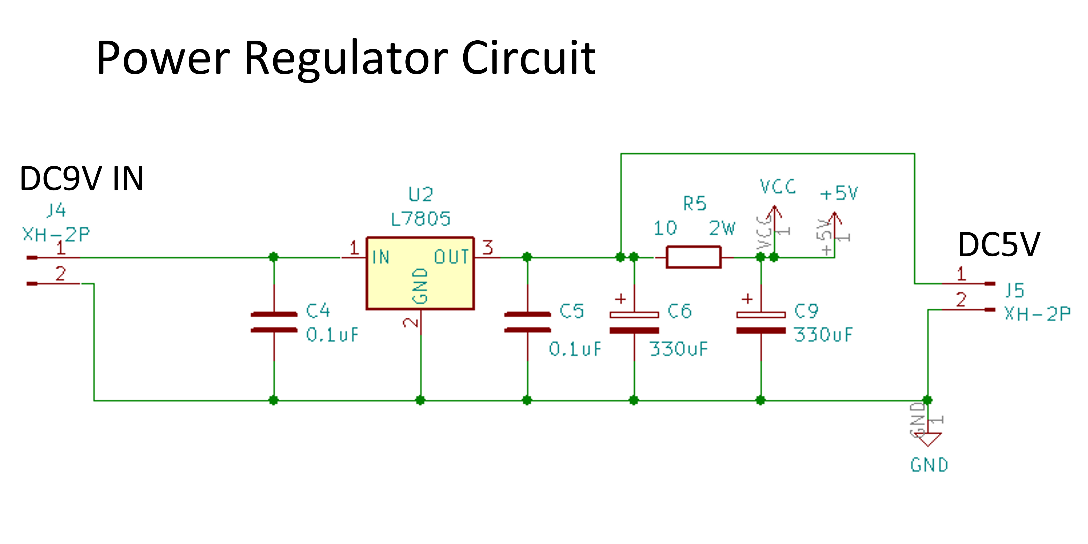
The circuit is a general circuit of a 3-terminal regulator. C4 and C5 are anti-oscillation capacitors. C6 is for ripple removal. It is also an RC low-pass filter for R5 and C9.
Regulator IC 5V1.5A TO-252 NJM7805SDL1

■ Main specifications
-Output method: Series
-Output positive / negative: Positive power supply
-Input voltage: ~ 35V
-Output voltage: 5V
-Maximum output current: 1.5 A
-Dropout voltage: 2.2V
-Allowable loss: 1190mW
-Ripple removal ratio (PSRR): 78dB
-Package: TO-252
** Quoted from Akizuki Denshi **
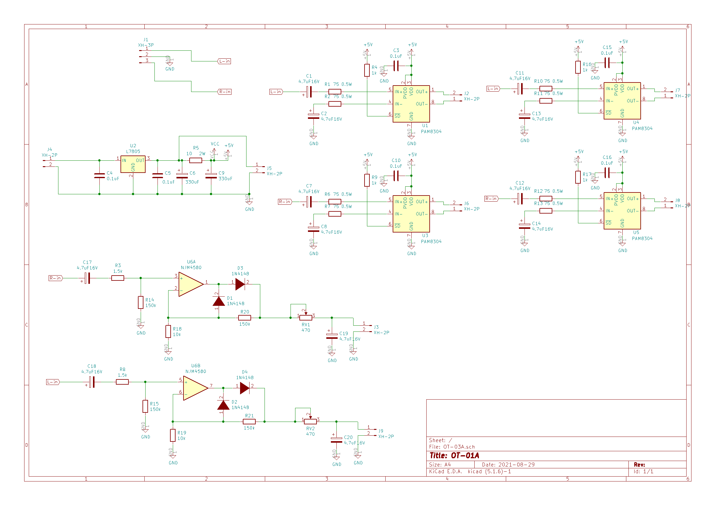
Finally, the entire schematic is shown.
Next time, we will design the board for this circuit.
